In-depth profile of KLA Corporationin Ann Arbor's tech ecosystem
KLA is the quiet giant of the Ann Arbor semiconductor scene. The company's Research Park Drive campus builds the inspection and metrology tools that every leading-edge fab on Earth uses to hunt defects at the nanometer scale. If a wafer is being etched at TSMC, Samsung, Intel, or Micron, there is a very good chance a KLA system built or designed in part in Ann Arbor is watching it happen.
The Ann Arbor site focuses on optical and e-beam inspection platforms, overlay metrology, and the image processing and machine learning pipelines that turn terabytes of raw wafer data into actionable defect maps. The engineering problem is brutal. You are looking for flaws the size of a few hundred atoms on a wafer that is moving across a stage, in a clean room, through optics that cost more than a house. The teams here employ physicists, optical engineers, ML researchers, and deeply specialized software engineers.
KLA's presence is a signal about how Ann Arbor fits into the semiconductor renaissance. The 2022 CHIPS Act, record capex from the hyperscalers, and the AI compute buildout have sent hiring demand for semiconductor talent to levels the industry has not seen in decades. KLA's Ann Arbor campus sits at the center of that demand, with direct recruiting pipelines into U-M's electrical engineering and applied physics programs.
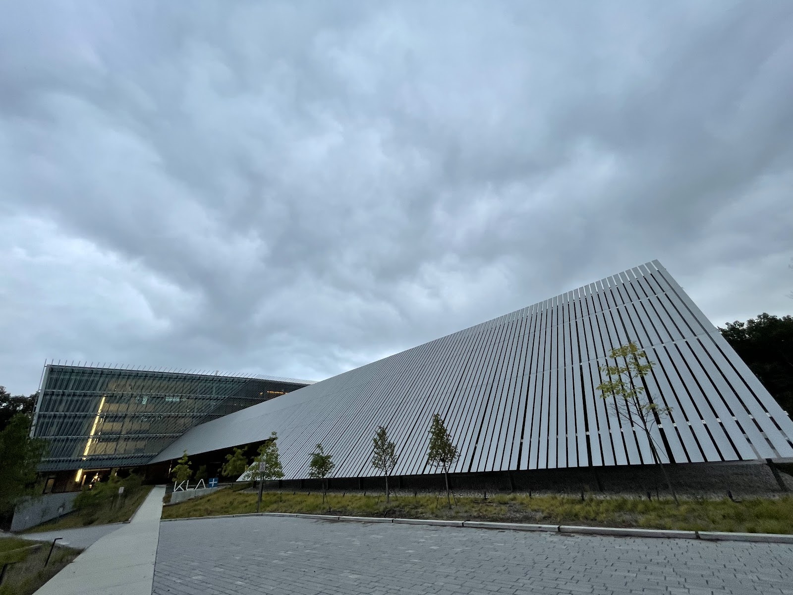
The site is in the southeast tech corridor off Eisenhower Parkway, a short drive from I-94 and the Ann Arbor Municipal Airport. Employees tend to cluster in Pittsfield Township, the Arbor Hills neighborhood, and the Saline school district. The commute to downtown is ten minutes. Airport access to California fabs and Taiwan suppliers is an hour to Detroit Metro. For a semiconductor engineer who wants to build frontier tools without paying Bay Area rents, this is one of the best addresses in the country.


